(Auszug aus der Pressemitteilung)

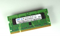
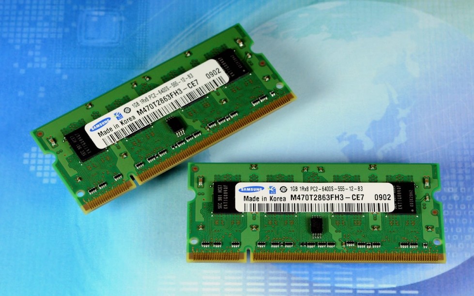
Seoul, Korea, February 4, 2009 – Samsung Electronics Co., Ltd., the world leader in advanced memory technology, announced today that it has developed and validated the first 40-nanometer (nm) class DRAM chip and module. This
Validation program for use with the Intel® GM45 series Express mobile chipsets.
„We accentuate our commitment as technology leader to deploying the most
efficient means in the DRAM business“ said Gerd Schauss, Director of Memory
Marketing, Samsung Semiconductor Europe. „For this we are using the most
innovative technology and system/platform validated operability“.
The migration to 40-nm class process technology is expected to accelerate
the time-to-market cycle by 50 percent – to just one year. Samsung plans to
apply its 40-nm class technology to also develop a 2Gb DDR3 device for mass
production by the end of 2009.
The new 40-nm class process technology will drive further reductions in
voltage against a 50-nm class device, which Samsung expects to translate
into about a 30 percent power savings
The finer DRAM technology node also delivers an approximately 60 percent
increase in productivity over 50-nm class process technology.
In addition, Samsung expects that its 40-nm process node will mark a
significant step toward the development of next generation, ultra-high
performance DRAM technologies such as DDR4.


Neueste Kommentare
24. April 2025
24. April 2025
18. April 2025
15. April 2025
14. April 2025
14. April 2025